Annotation
Wearable computing places tighter constraints on architecture design than traditional mobile computing. The real Structme of the computer is much more complicated than the structure of mobile computers. In modern computers, in particulm personal computers, there is increasingly a departure from the traditional architecture of von Neumann, due to the desire of developers and users to improve the quality and performance of computers. The quality of a computer is Chmacterized by many indicators. Tlus is a set of commands that the computer is able to understand, and the speed of the CPU, the number of peripheral I/O devices connected to the computer at the same time. The main indicator is the speed - the number of operations that a processor can perform per unit of time. In practice, the user is more interested in the performance of the computer - the indicator of its effective speed, that is, the ability to not just quickly function, but quickly solve specific tasks.The architecture is described in terms of miniaturization, power - awmeness, global low - power design mid suitability for an application. A system - in - a - package (SiP) generally contains a variety of systems such as analog, digital, Itigh frequency and micro electro mechanical systems, integrated in a system - level package connected through a substrate. In this article we propose a SiP model and the packaging implementation of the SiP as a complete microsystem.
Introduction
In now a days many sensor systems exist in the world, you can find them everywhere around us. The sensors are the connection between the real and the virtual world. These systems can exist in different forms and dimensions. But the sensor systems made to be integrated in the cloths have to be designed by the criteria of wearability. Those wearable sensor nodes have to observe and recognize the activities and the environment of the object. For this reason, miniaturized low - power signal processing algorithms have to be implemented to run in real - time at low power levels. Wearable computing is the missing part between the human world and the existing mobile devices.
The development of the wearable computing and the microelectronic technology require a new design of the Sensor Button, including future miniaturization, new components and more sensor integration, with complete covering of the criteria of wearability. To achieve a new complete context recognition system, new motion sensors have to be added. In this direction, Sensor Button 2 is able to integrate more motion sensors and the possibility to have physiology sensing. This Sensor Button 2 allows making one big step toward to the future of the wearable computers, a step to one complete, fully integrated, MCM based / Multi Chip Module/ system.
In this new version of Sensor Button, we focus the attention in the sensor integration (sensors per metric unit). With this criterion of measure, we can evaluate and show the future development of the wearable sensor systems. The sensor integration in the wearable systems depends mostly of the development of the sensors and the complexity of the recognition tasks. The simple dependency, more sensors - more possible activities to be recognized, pushes a lot of organization to focus of development of these systems.
The small, low power, on - body networks allow a real time observation of the object. For this reason, these on - body networks have to be always on, to provide useful information for the behaviour, the activities and the environment in different subjects.In this way one system combination of accelerometer, magnetic field sensor, gyroscope and microphone could be used for complete 3D recognition of the activities (hand moving, going upstairs, going downstairs, running etc.).
System Design
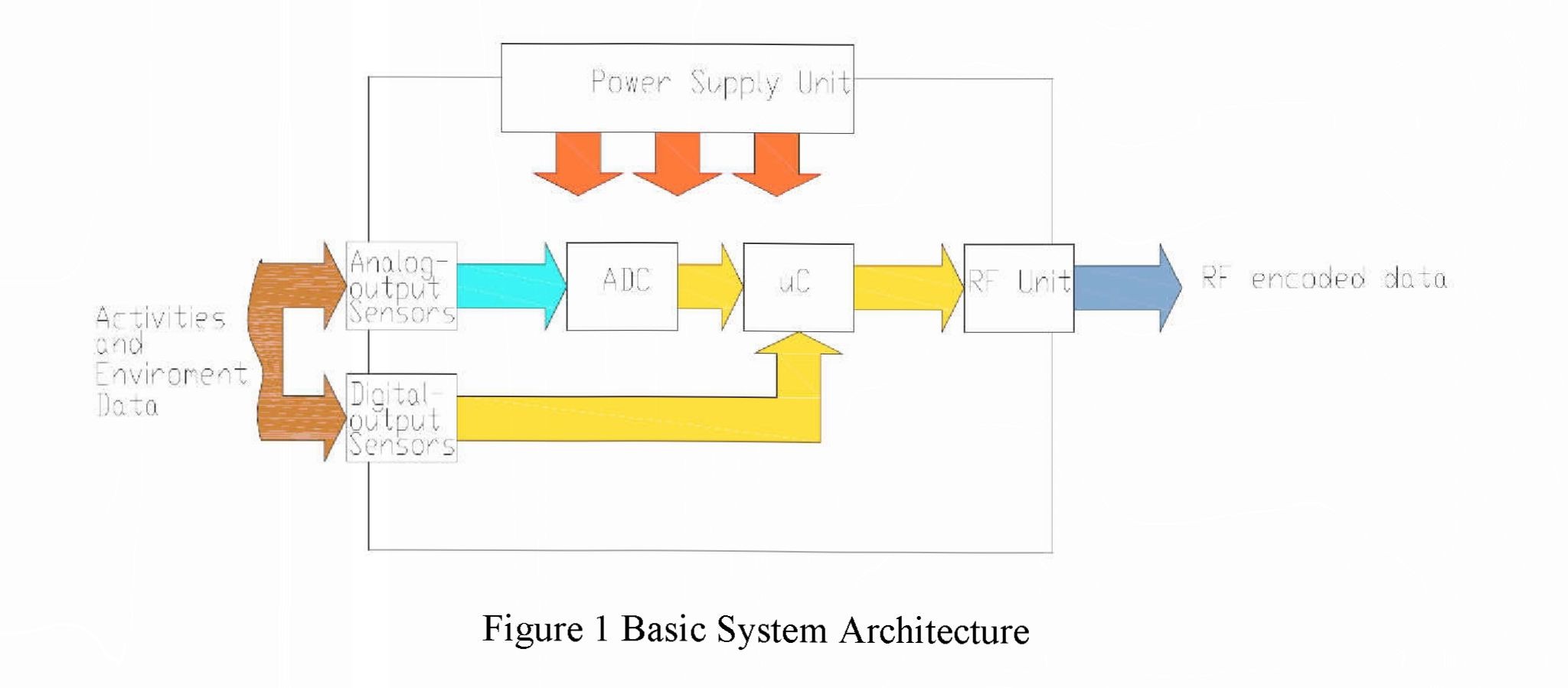
The design of Sensor Button 2 (Figure 1) consists of three principal subsystems: MCU/RF Unit (Microcontroller and Radio Frequency Unit), Sensors and Power Supply Unit.
MCU/RF Unit is a CC2430 Wireless microcontroller with combination in one system on chip the tree existing subsystems on the diagram - Analog - to - Digital Converter /ADC/, Microcontroller/uC/ and Radio Frequency Unit /RF Unit/.
- Microcontroller core in CC243 is an industry - standard enhanced 8051 MCU, 128 KB flash memory, 8 KB RAM, 12 - bit /VDC with up to eight inputs and configurable resolution, Two powerful USARTs with support for several serial protocols and 21 general I/O pins, two with 20mA sink/source capability.
- Radio Frequency Unit is a 2.4 GHz EEEE 802.15.4 compliant RF transceiver. The transmission output power is software configurable for up to 16 power levels.
- Sensors
Motion Sensor AMI601 integrates a 3 - axis magnetic sensor and a 3 - axis accelerometer with their controller IC in a single small package. The 3 - axis magnetic sensor consists of 3 magneto - impedance sensor elements set in mutually orthogonal position. The 3 - axis accelerometer consists of three sets of a magneto - impedance sensor and a micro magnet on a cantilever to detect acceleration, with the three sets in mutually orthogonal position.
The controller IC of the AMI601 consists of a circuit for detecting the magnetic signals from the 6 MI - sensor elements, an amplifier capable of compensating each sensors offset and setting appropriate sensitivity values, a temperature sensor for measuring the ambient temperature, a 12bitAD converter, an I2C serial output circuit, a constant voltage circuit for power control and a 8032 micro - processor controlling each circuit.
Integrated Dual - Axis Gyro IDG - 300 is an angular rate sensor (gyroscope). It uses InvenSense’s proprietary and patented MEMS technology with vertically driven, vibrating masses to make a functionally complete, low - cost, dual - axis angular rate sensor. All required electronics are integrated onto a single chip with the sensor.
 The IDG - 300 gyro uses two sensor elements with novel vibrating dual - mass bulk silicon configurations that sense the rate of rotation about the X - and Y - axis (in - plane sensor elements with novel vibrating dual - mass bulk silicon configurations that sense the rate of rotation about the X - and Y - axis (in - plane sensing). This results in a unique, integrated dual - axis gyro with guaranteed - by - design vibration rejection and high cross - axis isolation.
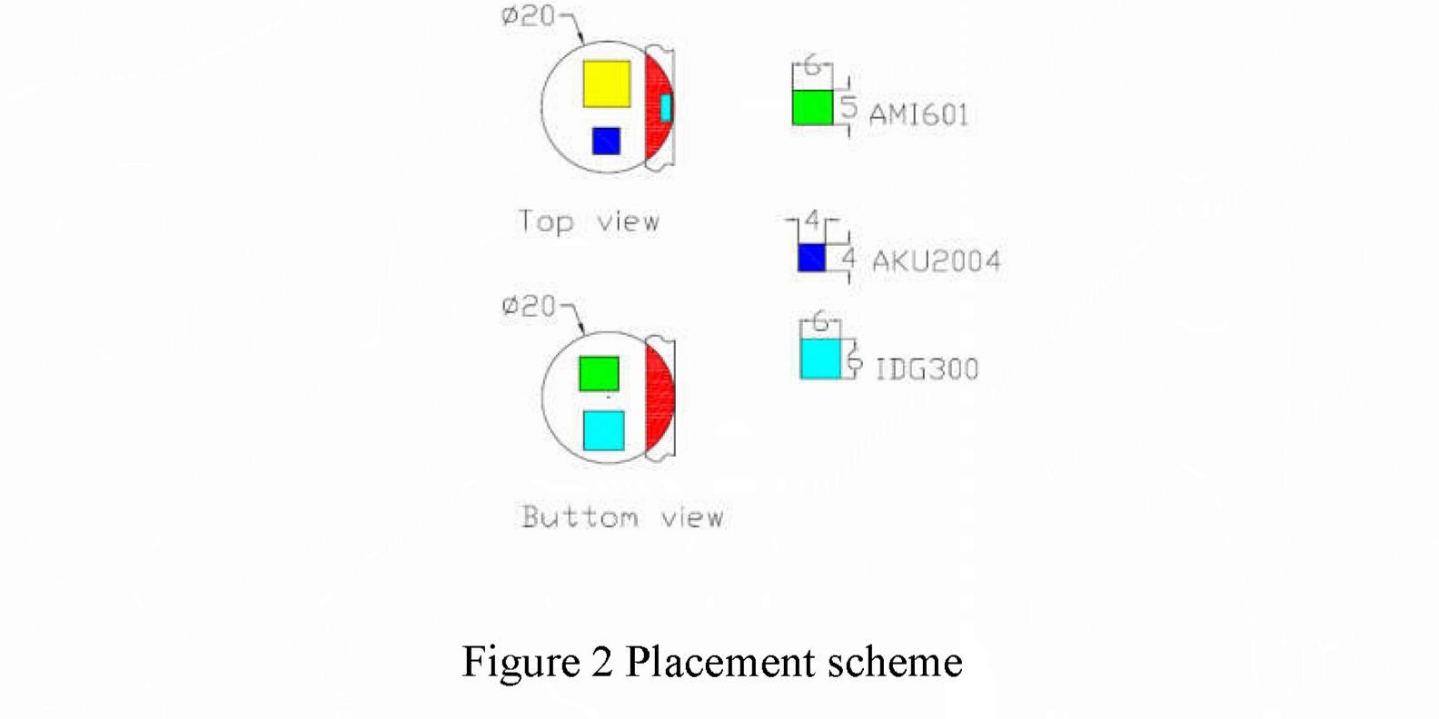
The IDG - 300 gyro includes integrated electronics necessary for application - ready functionality. It incorporates X - and Y - axis low - pass fdters and an EEPROM for on - chip factory calibration of the sensor. Factory trimmed scale factors eliminate the need for external active components and end - user calibration.
The scale factor of the gyroscope depends on the amplitude of the mechanical motion and the trim setting of the internal programmable gain stages. The oscillation circuit precisely controls the amplitude to maintain constant sensitivity over the temperature range.
Microphone AKU2004 is a surface - mountable CMOS MEMS Digital - Output Microphone which is ideal for use in microphone array applications where a high degree of noise immunity is required. The AKU2004 integrates an acoustic transducer, analog output amplifier, and a 4th_order sigma - delta modulator on a single chip. The output of the microphone is pulse density modulated (PDM); a single - bit digital output stream that can be decimated by a digital filter in downstream electronics. The digital output is more robust than the low - level analog output signals of the standard ECM and therefore saves significant time and expense in system design and eliminates the dependence on shielded cables for signal routing.
Power Supply Unit combines battery and low voltage boost converter TPS61201 from Texas Instruments. The amount power consumption is calculated in the base of absolute maximum ratings of the components. The average maximum peak current consumption is 40mA.
The power consumption will be reducedby the optimization of the appropriate working algorithm. Because of the digital output sensors, feedback from the microcontroller allows to be madeinstate of the continuous working time of the sensors.
Whysysteminapackage? "
Most of the electronic packaging modules require low cost, high performance, high speed, good manufacturability, environmental compatibility last but not the least, long term reliability. In a System - in - a - Package (SiP) normally the objective is to combine many or all of the electronic requirements of a functional system or subsystem into one package. Within a great variety of SiP’s, we focus on SiP’s which size ranges from several centimeters to one millimeter or even smaller. The system may include a diversity of components like passives, RF shields, connectors, solar cells, batteries, micro power generators etc.
A SiP package differs with a system on Chip (SoC) technology [2] where all the functionalities of the system are realised on a single chip as. SiP has the advantage that each
IC can be optimised for its function in terms of design, and wafer fabrication process. Generally using a SiP solution has the following advantages from the design point of view.
- SiP solutions often have reduced routing complexity and layer count. It is possible to move the routing from the motherboard to substrate. Especially in complex designs this saves the time during the design phase.
- SiP solutions allow reducing the power consumption by shortening the line lengths between IC’s, which in turn reduces the capacitive load.
- With in a SiP it is often possible to place memory and logic chips close to each other, allowing to increase the data speed enhancements from an ASIC (Application - Specific - Integrated - Circuit) or CPU (Central - Processing - Unit) to memory.
- In RF (Radio Freequency) and wireless SiP, package is treated as a part of the circuit, which makes it possible to enhance the circuit function through the package design and materials selection.
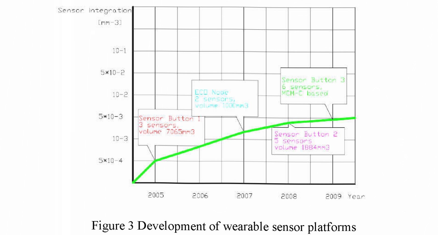
One of the most important criteria to evaluate the existing sensor platforms is the sensor integration. In term of wearable computing we use the sensor integration in meaning of sensors per mm3 . To show the future development of the wireless sensor platforms and to situate the Sensor Button 2, we made this graphic in base of some existing platforms.
From Figure 3 we can see the evolution in the wireless sensor systems. The next step for our research will be a MCM based Sensor Button.
Miniaturization of the system
The wearable sensor nodes should be extremely small and consume so little power that no power source change is required for several months to years. Working towards this vision, the previous work dealt with issues such as [1], activity recognition using low - power features and classifier algorithms, optimization of power and size in a multi - sensor context recognition platform, development of hybrid micro power supply to achieve autonomous behaviour, reliability modelling of embedded systems in wearable computing, detailed systematic approach considering wearability and power consumption for selecting optimized architectures with respect to power consumption.
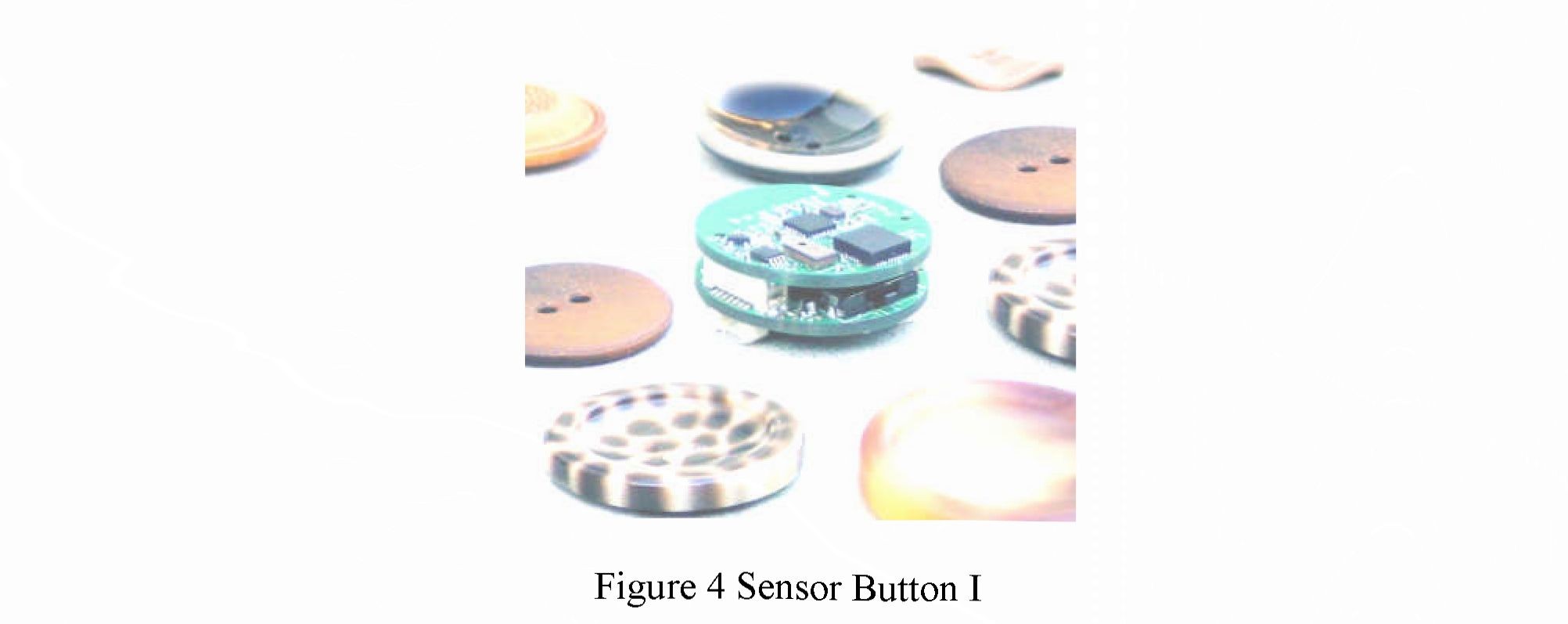

The first sensor button system consisted of a number of different modules, assembled in one package. The elements of this module were: sensors / including analog output and digital output sensors /, analog to digital converter (ADC), microcontroller (uC), radio frequency unit (RF Unit) and power supply (Figures 1 and 4).
The presented sensor button II (Figure. 5) enlarges the number of activities to be recognized (identified) and is miniaturized in 3D. A motion sensor (3 - axis magnetic sensor and a 3 - axis accelerometer) and an integrated dual - axis angular rate sensor (gyroscope) are included in the system and a microphone as well. The next step is to add a physiological sensing.
In Figure 1 we can see also the division of two ways of sensing - sensors with analogue outputs and sensors with digital outputs. This division based on the sensor progress has the tendency of miniaturization of the analogue part. The miniaturization of the analogue part minimizes the power consumption and in the same time simplifies the required amplifiers and analogue to digital converters [7]. The new concept of wireless microcontrollers combines the radio frequency /RF/ Unit and the microcontroller core. This provides possibilities for integration of more functions in one package. The dimensions of Sensor Button II (Fig. 5) are: diameter 25 mm, thickness: ~6mm. The criteria of «wearability» and functionality will be completed with the possibility of integration in a MCM.
Conclusion
The new Sensor Button represents one complete, wearable system with large recognition possibilities. This new version gives the possibilities to study a huge number of activities. This version gives the bases of the new era in wearable sensor platforms - the Sensor Button implemented as a SiP.
We are focusing our attention now in the thermal design and optimisation of the Sensor Button.
Literature:
- Bharatula N. B.. Lukowicz P., Troster G.: Functionality - Power - Packaging Considerations in Context Aware Wearable Systems. In: 9thIEEE International Symposium on Wearable Computers, ISWC 08'. Osaka, Japan. (2008) 197- 198.
- Tununala R.: Introduction to System - On - Package, McGraw - Hill, 2007, ISBN: 0071459065.
- Texas Instruments, http://www.ti.com/ (2007).
- InvenSense. http://www.invensense.com/ (2007).
- Aiclii Micro Intelligent Corporation. http://www.aichi - mi.com/ (2007).
- Akustica digital microphones, http://www.akustica.com/ (2007).
- Morris J.. Nanopackaging: Nanoteclmologies and Electronics Packaging. Springer, 2018, Second Eddition.